


Total Semiconductor Solution Material
Products

TAPE
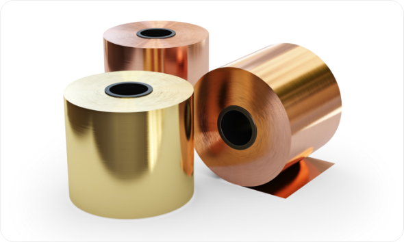
Sputtering Tape for EMI Shielding
Product Description
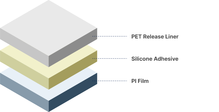
Uses a silicone-based adhesive to provide stable properties in processes that require high heat resistance.
Structure
Features

Temporarily fixes packages during the sputtering process for the EMI shielding layer.

Provides heat resistance up to 400°C.

Low outgassing.

Maintains strong adhesive strength even above 200°C.

No residue after 2 hours at 200°C.
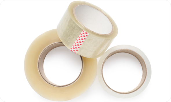
UV Curable Sputtering Tape for EMI Shielding
Product Description
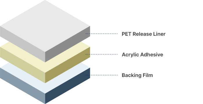
Tape that can be easily removed by exposure to UV light.
Structure
Features
Temporarily fixes the package during the wafer grinding process after EMI Shielding deposition

Excellent lamination performance (Good Ball Dipping, minimized voids)

Excellent sawing characteristics

Easy package (PKG) pick-up
No residue after removal
QFN Backside Tape
Product Description
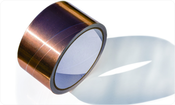
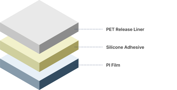
A tape applied to the backside of the lead frame to prevent resin leakage during the molding process.
Structure
Features
Provides high thermal stability during the molding process.
No mold flash and low outgassing properties.
Excellent processability and workability with no residue remaining.

High modulus enables stable wire bonding during pre/post-tape processes.
UV Curable Package Dicing Tape
Product Description
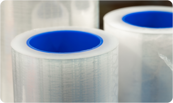
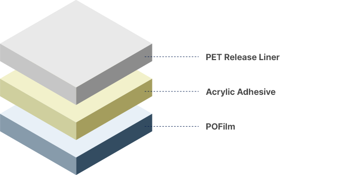
Provides high adhesion to firmly secure the wafer during the dicing process.
The adhesive strength decreases after UV irradiation, allowing for easy removal of the packages.
Structure
Features

High adhesion for package stability during dicing.
Easy package pick-up due to reduced adhesion after UV irradiation.

No residue or contamination after curing.

- Business Registration Number 135-86-06809
- E-mailsjjung@11electron.com
- Address401, Building 3, Innoflex, 304 Sinwon-ro, Yeongtong-gu, Suwon-si, Gyeonggi-do, Republic of Korea
- Tel031-8019-8999
- Fax031-8019-8997